Use an op amp and a dual SPST to switch signals under digital control.Many applications require a method of switching an analog or a digital signal on or off under digital control. A "wish list" of specifications for such a switch might include attenuation of less than 90 dB when the switch is in its off-state, distortion of no more than 0.002% when the switch is in its on-state, and the ability to respond to an on or an off command in 10 µsec or less. In addition, the circuit should accommodate positive- or negative-going signals, and no turn-on or turn-off overshoot should occur for either signal polarity. The list might also require that the circuit's control input must accept digital signals from most logic families and that the circuit's SNR should exceed 90 dB. The circuit in Figure 1, comprising IC1, a low-noise, high-speed, precision Linear Technology LT1007 operational amplifier and IC2, a Maxim MAX301 dual SPST, normally open analog switch, fulfills these requirements. In the circuit, VIN is the input voltage, and VOS and IOS represent operational amplifier IC1's voltage and current offsets of either polarity. IOFF represents the off-state leakage current of either section of analog switch IC2. In the buffer circuit, R=R1=R2, and R4=R/2. Hence, ΔR=(R1×R2)/(R1+R2)–R4. If all resistors were identical in value, ΔR would equal zero. However, each resistor exhibits its own tolerance error, and the equation for ΔR expands to:

where e1 through e4 are maximum tolerance errors of ±1%. Worst-case values for ΔR occur when the tolerance values e1 and e2 for R1 and R2 are of the same sign and e4 for R4 has the opposite sign:
Simplifying further, ΔR=±R|e|}=±{(0.01)R} when you use 1%-tolerance resistors for R1, R2, and R4. The combination of the resistors' tolerances with the operational amplifier's internal errors and leakage effects from switches IC2A and IC2B determines the buffer's accuracy. When the circuit is on, both IC2A and IC2B are open. The following equation defines the circuit's output voltage:
Simplifying further, you can calculate VOUT(ON) as: VOUT(ON)=–(VIN)+VOS+((IOS)×(ΔR))+((IOFF)×(R)). Most of today's solid-state switches present an IOFF of less than 1 nA, and you can select an op amp for IC1 whose VOS is less than 50 µV and whose IOS is less than 50 nA. Thus, for the resistor values in Figure 1, the maximum error for the amplifier's on-state is approximately 80 µV, or 0.0008%, when referred to a 10V nominal output. You can determine the minimum allowable value of the amplifier's load resistance by solving the following equation:
where VSAT represents the op amp's maximum saturated output voltage—usually, 13.5V for ±15V power-supply voltages. For example, using the resistor values in Figure 1 and assuming a maximum output voltage of 10V, you can calculate a minimum allowable load resistance of 3.3 kΩ. Also, IAMP, the current from IC1, should be less than the device's specified maximum current output: IAMP=(VOUTMAX)×[(1/R2)+(1/RLOAD)]. Using these values, you can determine that IAMP is 3.5 mA, which is less current than most op amps as sources deliver. When the amplifier is off, switches IC2A and IC2B are closed. In this state, the worst-case output occurs for VINMAX. IC1's offset errors are negligible with respect to the full-scale input voltage. Therefore, for the real case in which the on-resistance of IC2A and IC2B is much less than the load resistance, the following equation defines the circuit's output voltage: VOUTOFF=–[(VIN×R2×RON×RON)/(K1+K2+K3–K4)], where K1=R1×R2×R3, K2=R1×R3×RON, K3=R1×RON×RON, and K4=R1×R2×RON. For R1=R2=R and RON<<R, and RON<<R3, the equation simplifies to: VOUTOFF=–[(VIN×RON×RON)/(R×R3)]. Many of today's analog switches present a maximum 20Ω on-resistance, and, using the resistor values in Figure 1 and an input voltage of 10V, you can calculate that output voltage to be approximately 200 µV, or 0.002%, when referred to a 10V nominal output. Amplifier IC1's slew rate limits the circuit's dynamic behavior, because analog switch IC2 generally switches in much less than 1 µsec. Using an operational amplifier with a slew rate of 1.5V/µsec yields a circuit-response time of 10 µsec. For applications that require unipolar outputs when the amplifier is in its off-state, you can add a known output-offset voltage by connecting resistor R5 between the buffer's output and the power-supply voltage of the same polarity as the desired offset voltage. Note that IC1's output must be able to sink current. Adding resistor R5 doesn't affect the circuit's output voltage in its on-state because the closed-loop gain lowers the amplifier's output impedance. To analyze the circuit's offset output voltage, assume that IC2A and IC2B present an on-resistance that's much less than RLOAD, R2, and R5. The following equations define the circuit's positive and negative offset-output voltages, VOUT(OS) and –VOUT(OS), respectively:
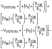
To make the offset voltage less dependent on the input signal, calculate the maximum value for R5 as:
Using the resistor values in Figure 1, solving this equation produces a minimum reliable offset voltage of 2 mV; the value of R5 must be 150 kΩ or less. The maximum current-sinking ability of IC1 determines the minimum value of R5. |
|


